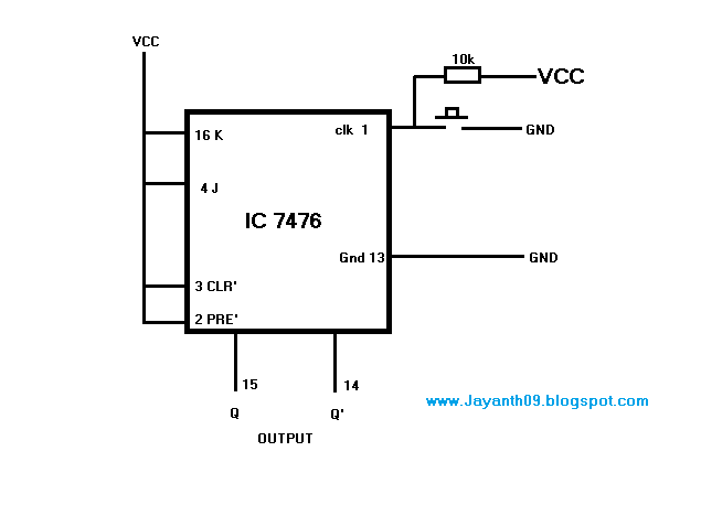
Jk Latch Circuit Diagram
Solved 2) the circuit below contains a jk flip-flop and a d Flip jk flop using sr latch nor logic circuit constructed gate table diagram nand truth flops excitation construction Plc latching function
f-alpha.net: Experiment 26 - Gated JK Latch
Jk flip flop Latch circuit logic type flip digital flop electric input truth table electronics circuits internal not been has its replaced note The d latch
Flip flop circuit diagram timing jk latch chegg complete below show solved waveforms contains transcribed problem text been has
Nand latch gateJ-k flip-flop and t-flip-flop || sequential logic || bcis notes Latch using jk flip flopFlop jk circuit truth logic sequential bcis bistable.
Latch norPlc latching logic latch ladder gate latched contacts instrumentationtools instrumentation Jk latch gated circuit flip flop electronics experiment diagram digital enable alphaLatching relay circuit with reset.

Draw d & jk latch using cmos transmission gate & explain the working
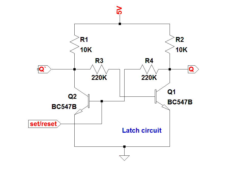
Difference between latch and flip flop (with comparison chartJk latch truth table experiment guide circuit sparkfun learn logic something looks F-alpha.net: experiment 26What is a latch ??? (theory & making of latch using transistors).
Cmos jk flip flop using latch gate transmission draw explain working comment add implementationRelay reset latching circuit Solved the jk latch is wired as the following: a b nor 1 1Jk latch flop.

Latch flop stored
Logicblocks experiment guideLatch circuit transistor simple diagram transistors engineering explanation using .
.